The output value of the $ 46 billion global printed circuit board (PCB), about 14% of Taiwan businessmen output value accounted for one quarter of the global output, if combined with the mainland output value, up to four percent of the global output, the output value of the two sides of theso, in addition to the information board, communication board presentation huge growth in the industry continue to amplification. Often within the printed circuit board generally are plywood, drilling and copper circuit is turned on, however, the traditional mechanical drilling and laser drilling, perforation (Through Via) and blind hole (Blind Via) residual glue residue (smear) or fiberglass, covered metal layer and affect the conduction of the circuit. Traditional way to clean multi-acid such as potassium permanganate glue residue removal, except drilled aperture shrinking and fine acid fear, because of the surface tension and can not enter the hole for cleaning; Secondly, the wet -process liquid waste will be accompanied by the pollution problem, a large number of human demand and consumption of liquid acid; addition, some special plates, such as communication boards use Teflon plate, plate for pH more passivation, so wet process and not be able to effectively remove the glue residue Seen in this light, the dry plasma cleaning process will gradually receive much attention. Taiwan's main plasma technology plant-XX technology was a few years ago to develop the only integrated high-voltage electric field strength, ICP (inductively coupled plasma), the HCP (hollow cathode plasma) plasma ashing residue machine which can effectively deal with the residue of glue the perforation and blind hole, while the cost of the gas consumed in the plasma process is very suitable for soft, hard board, even the hard and soft composite board at the glue residue to the adhesive residue, activation, crude and application of the cleaning process.
Plasma / plasma rapid rise in recent years, become the driving force behind the industrial revolution. Not only has become the field of semiconductor process indispensable tool, while other areas, such as optoelectronics, IC packaging, printed circuit board, biomedical, 3C products and traditional industries, but also enhance the technology and added value of the weapon.
Can be seen from the surface of the component analysis can be quite good to glue residue after control of plasma / plasma processing parameters.
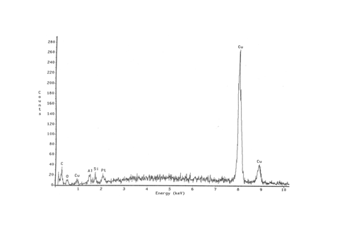
C
|
O
|
Si
|
Cu
|
Al
| |
No Plasma Desmear
|
39 %
|
2.6 %
|
0.8 %
|
56.5 %
|
1.1%
|
C
|
O
|
Si
|
Cu
|
Al
| |
Bad Cleaning Effect
|
20.4 %
|
1.3 %
|
0.7 %
|
76.4 %
|
1.2 %
|
Good Cleaning Effect
|
0 %
|
12.6 %
|
0 %
|
87.4 %
|
0 %
|
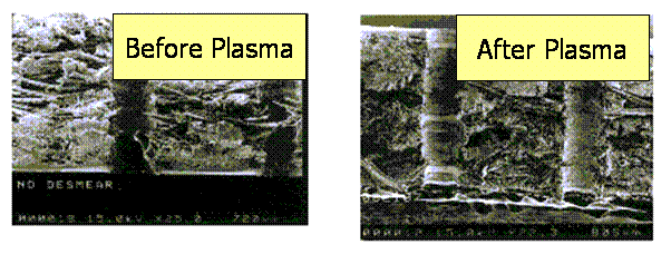
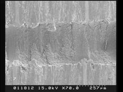
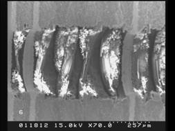
Also observed differences in plasma / plasma to go before and after the glue residue from the hole slice in plasma / plasma ashing slag processing can clearly see the copper layer covered bare, while the circuitafter plasma treatment, the plate will be accompanied by surface roughening effect, there is a considerable degree of improvement for the quality of the post-process copper.
↓
↓

↓

(Surface roughness before) → plasma Desmear

PCB board holes into the hole more common to have the image into a hole, dry or wet erosion, laser drilling and punching, which is based on laser into the hole with the image into the hole as the most important technology. But often have peeling, dust pollution generated in the production process of the images into a hole, so the proportion of decreasing, while the quality of the laser into a hole, and also has a considerable number of advantages, but its largest shortcomings in addition to the equipment is very expensive, the outer edge of the drilled hole often rugged phenomenon need to do additional processing and drilled aperture limited; while the Company by plasma etching into the hole required low equipment costs, and because the process is performed in the vacuum environment, so opposite to reduce pollution caused by the IC element. Known in the production process of the wafer (wafer), plasma etching steps well into the sub-micron (sub-micron). So, when drilled aperture 3 mil or less than 3 mil, will take advantage of the plasma drilling technology, the development of this technology not only applies to tiny aperture of drilling, and etching through the semiconductor polishing (photolithography) a combination of technology, will be up to the fast and high-density printed circuit board drilling technology, while at the same time the use of plasma drilling drilling holes fairly flat, do not have to do any post-processing, and very cost-effective. Throughout, Plasma drilling technology will have the following advantages:
(1) The high precision of the hole.
(2) the formation of holes around the high.
(3) drill smaller aperture.
(4) the etching rate is fast, can be a large area.
(5) This equipment than the laser into the hole device low cost.
(6) The vacuum plasma can be avoided due to the laser drilling brought bromine, dioxin and other gases harmful to the human body directly exposed to the body around.
Plasma drilling technology has 4 high 2 micro-features (high-precision, high flatness, high uniformity, high capacity, small aperture, micro cost), and at the same time one can handle multi-
Piece of large-size panels, the relative expensive and handle aperture limited laser drilling techniques is one of the solutions may think of the next printed circuit board fabrication process.
沒有留言:
張貼留言